Example explanation of NAND Flash principle and usage
Release time:2024-05-04 Number of views:3684This article takes Micron's MT29F2G08 as an example to introduce the principle and use of NAND Flash.
1. Overview
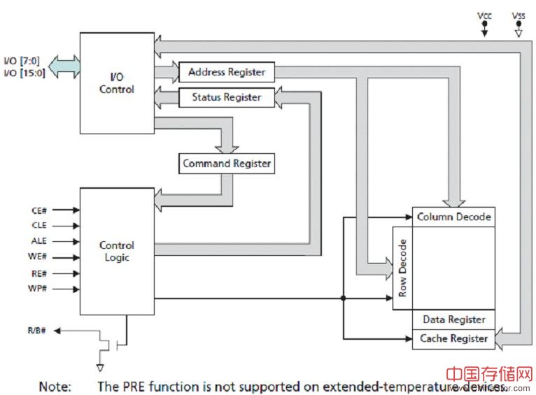
MT29F2G08 uses a highly reusable 8-bit bus (I/O [7:0]) to transmit data, addresses, and instructions. Five command pins (CLE, ALE, CE #, WE #) implement the NAND command bus interface protocol. Three additional pins are used for: controlling hardware write protection (WP #), monitoring chip status (R/B #), and initiating power on automatic read features (PRE - only supported by 3V chips). Note that the PRE function does not support wide temperature chips.
MT29F2G08 has 2048 erasable blocks internally, each divided into 64 programmable pages, each containing 2112 bytes (2048 bytes are used as the data storage area, and 64 spare bytes are generally used for error management).
Each 2112 byte page can be programmed within 300us, and each block (64x2112=132K) can be erased within 2ms. The on-chip control logic automatically performs Program and ERASE operations.
The internal storage array of NAND is accessed on a page basis. When reading, a page of data is copied from the internal storage array to the data register, and then output in byte order from the data register. When writing (programming), it is also based on pages: after the starting address is loaded into the internal address register, the data is sequentially written into the internal data register. After the page data is written, the array programming process starts.
In order to increase programming speed, the chip has a CACHE register. In CACHE programming mode, data is first written to the CACHE register and then to the data register. Once the data is copied into the data register, programming begins. After the data register is loaded and programming begins, the CACHE register becomes empty and can continue to load the next data. This allows for parallel programming and data loading, improving programming speed.
The Internal Data Move command also uses internal CAHCE registers, which usually take a long time to move data. By using internal CACHE registers and data registers, the speed of data movement is greatly increased, and external memory is not required.
2. Functional Block Diagram
3. Pins
| name |
type |
describe |
| ALE |
I |
Address latch enable. When ALE is high, on the falling edge of WE #, the address information is locked in the address register of the chip through I/O [7:0]. If the transmission is not address information, ALE should be low. |
| CE# |
I |
Film selection. Once the device enters the Program or ERASE operation, CE # can become invalid. |
| CLE |
I |
Command latch enable. When CLE is high, on the rising edge of WE #, the command is locked to the command register through I/O [7:0]. When no command is transmitted, CLE should be low. |
| PRE |
I |
Enable power on reading. |
| RE# |
I |
Reading enables. |
| WE# |
I |
Write enable. |
| WP# |
I |
Write protected. When it is low, all programs and ERASE are disabled. |
| I/O [7:0] |
I/O |
Data input/output. Transmit commands, data, and addresses. Only during read operations, data is output. |
| R/B#, R/B2 |
O |
Get ready/busy. Open collector output. An external resistor needs to be connected, and this pin indicates that the chip is undergoing a Program or ERASE operation. During the read operation, it indicates that data is being transferred from the array to the serial data register. Once these operations are completed, R/B # returns to the High-Z state. |
| Vcc |
source |
source |
| Vss |
land |
land |
4. Addressing
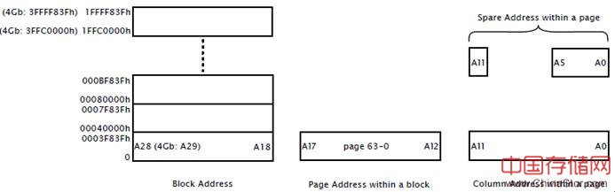
Block address and page address=actual page address. Through this diagram, we hope to understand block, page, block address, page address, column address, backup space, and backup address

| Cycle |
I/O7 |
I/O6 |
I/O5 |
I/O4 |
I/O3 |
I/O2 |
I/O1 |
I/O0 |
| 1 |
CA7 |
CA6 |
CA5 |
CA4 |
CA3 |
CA2 |
CA1 |
CA0 |
| 2 |
LOW |
LOW |
LOW |
LOW |
CA11 |
CA10 |
CA9 |
CA8 |
| 3 |
RA19 |
RA18 |
RA17 |
RA16 |
RA15 |
RA14 |
RA13 |
RA12 |
| 4 |
RA27 |
RA26 |
RA25 |
RA24 |
RA23 |
RA22 |
RA21 |
RA20 |
| 5 |
LOW |
LOW |
LOW |
LOW |
LOW |
LOW |
LOW |
RA28 |
CAx: Column address; RAx=Line Address
5. Bus operation
| CLE |
ALE |
CE# |
WE# |
RE# |
WP# |
PRE# |
MODE |
|
| H |
L |
L |
Rising edge |
H |
X |
X |
Reading mode |
Command input |
| L |
H |
L |
Rising edge |
H |
X |
X |
Address input |
|
| H |
L |
L |
Rising edge |
H |
H |
X |
Write Mode |
Command input |
| L |
H |
L |
Rising edge |
H |
H |
X |
Address input |
|
| L |
L |
L |
Rising edge |
H |
H |
X |
data input |
|
| L |
L |
L |
H |
Descending edge |
X |
X |
Sequential reading and data output |
|
| L |
L |
L |
H |
H |
X |
X |
During reading (busy) |
|
| X |
X |
X |
X |
X |
H |
X |
During programming (busy) |
|
| X |
X |
X |
X |
X |
H |
X |
During erasure (busy) |
|
| X |
X |
X |
X |
X |
L |
X |
Write protect |
|
| X |
X |
H |
X |
X |
0V/Vcc |
0V/Vcc |
Standby |
|
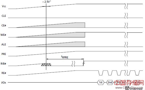
Power on automatic read: During power on, PRE is VCC, and the 3V VCC device automatically transfers the first page to the data register without issuing a command or address latch sequence. When the VCC reaches approximately 2.5V, the internal voltage detector triggers the power on automatic reading function. During the process of copying the first page of data to the data register, R/B # is low. After the copy is completed, R/B # becomes high. Under the action of the RE # pulse, the first page of data can be output sequentially.
6. Command Table
| operation |
Cycle 1 |
Cycle 2 |
Valid during busy periods |
| PAGE READ |
0x00 |
0x30 |
NO |
| PAGE READ CACHE MODE START |
0x31 |
- |
NO |
| PAGE READ CACHE MODE START LAST |
0x3F |
- |
NO |
| READ for INTERNAL DATA MOVE |
0x00 |
0x35 |
NO |
| RANDOM DATA READ |
0x05 |
0xE0 |
NO |
| READ ID |
0x90 |
- |
NO |
| READ STATUS |
0x70 |
- |
NO |
| PROGRAM PAGE |
0x80 |
0x10 |
NO |
| PROGRAM PAGE CACHE |
0x80 |
0x15 |
NO |
| PROGRAM for INTERNAL DATA MOVE |
0x85 |
0x10 |
NO |
| RANDOM DATA INPUT for PROGRAM |
0x85 |
- |
NO |
| BLOCK ERASE |
0x60 |
0xD0 |
NO |
| RESET |
0xFF |
- |
YES |
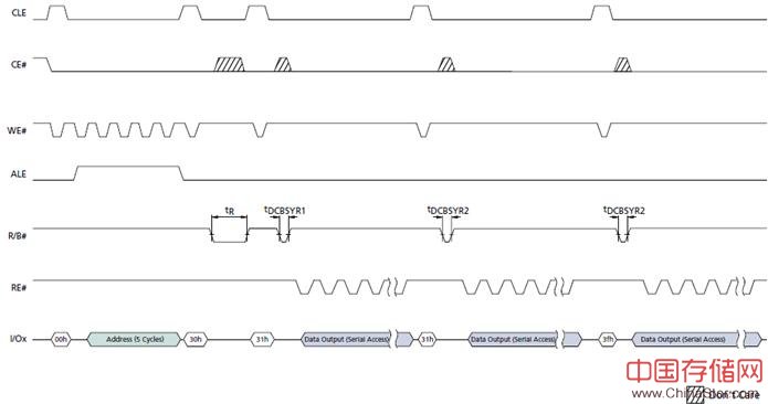
7. PAGE READ, 0x00-0x30
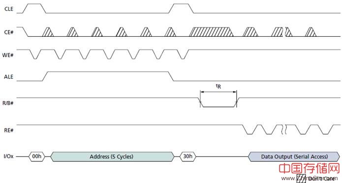
After 5 address cycles, the starting address for reading is determined. Under the action of the RE # pulse, the data is sequentially output from this starting address until the end of this page.
8. RANDOM DATA READ, 0x05-0xE0
Random data reading is to enable users to set new column addresses and increase the flexibility of data reading. The random reading mode is enabled after page reading (0x00-0x30 sequence). The number of times this command can be issued is unlimited. But only the reading of the current page data.

9. PAGE READ CACHE MODE START, 0x31; PAGE READ CACHE MODE START LAST,0x3F
After issuing the PAGE READ command, when R/B # increases, the 0x31 command is sent. At this time, the content of the data register is transmitted to the CACHE register, and the first PAGE READ command can be sequentially read from the CACHE register to obtain data. As this is a data register, it is useless. Therefore, the chip automatically starts the PAGE READ command to read the next page and read it to the data register. It can be seen that this improves the reading speed. Except for the first PAGE READ command, all other PAGE READ commands are automatically performed in the background. Use the 0x3F command again to prevent the chip from automatically issuing the PAGE READ command again.
10. READ ID, 0x90
Read the manufacturer's chip identification.

11. READ STATUS, 0x70
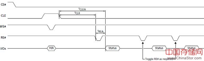
Read the 8-bit status of the chip. It can be read repeatedly through the RE # pulse.
12. Programming operations
PROGRAM PAGE 0x80-0x10:
Micron NAND FLASH only supports page programming. Within a block, pages must be continuously programmed from the low bit of a block to the high bit of that block, and programming with random page addresses is prohibited.
The chip also supports partial programming operations for pages, which means that any single bit can only be programmed once before requiring an erase. However, this type of page can be divided into allowing up to 8 programming operations before requiring an erase.
SERIAL DATA INPUT 0x80:
The PAGE PROM operation requires loading the SERAIL DATA PUT (0x80) command into the command register. After 5 address cycles, the serial data is loaded to the starting address of the value through continuous WE # cycles. The PROM (0x10) command is written after the data input is completed, and the internal write state cycle automatically executes the appropriate programming algorithm and controls all necessary timing programming and comparison operations. Writing comparison only checks whether "1" has been successfully programmed as "0".
During array programming (tPROG), R/B # is low. During programming operations, only the READ STATUS and RESET commands are valid. The status register Bit6 reflects the status of R/B #. When the chip is ready, the status of Bit0 is read to determine whether the programming operation is successful or failed. The command register remains in read status register mode until a new valid command is written.
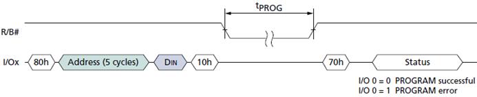
RANDOM DATA INPUT 0x85:
Initiate
Previous article: Introduction to SSD Trim Next item: No more Return to List
Contact us
Office address: Room 606, Tongfang chuangxiang commune, XINER Sports Center complex building, Xinqiao street, Bao'an District, Shenzhen
Hotline: 0755-27502764
National/enterprise level:135-1068-5504
188-9877-7001
Industry/Work Regulations:135-3095-1400
189-2939-2673
Mailbox:sales@pancunstorage.com
